CHIMERA Board
CHIMERA (Cubesat Highly Integrated MEmory Radiation Assurance) is an internal ESTEC (TEC-QEC/EDD) experiment planned for launch on 16th of August on board of GOMX-4B CubeSat. The goal of the experiment is to test in-space COTS SPI memories. Twelve memories were selected for that (three of each will fly): LE25U40CMC (ONSemi FLASH ), FM25W256 (Cypress FRAM), 23LC1024 (Microchip SRAM), N25S830H (ONSemi SRAM). In-space testing includes monitoring the number of SEUs/MBUs, SEFIs and Latch-Ups.
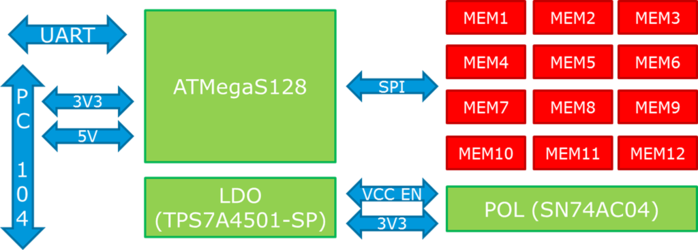
The CHIMERA board has PC104 CubeSat format and can be divided into two parts: radiation tolerant monitoring circuit and array of twelve memories under test - Figure 1 shows the block diagram. The board requires low resources: mass is 60.8 gr, power consumption of 62mW nom. and produces 10kB of telemetry per day.
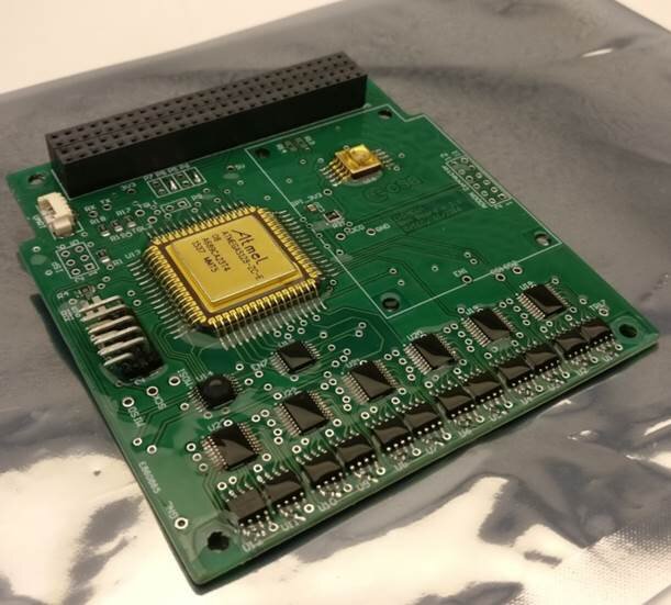
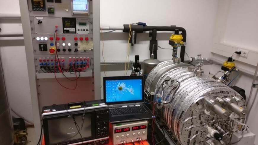
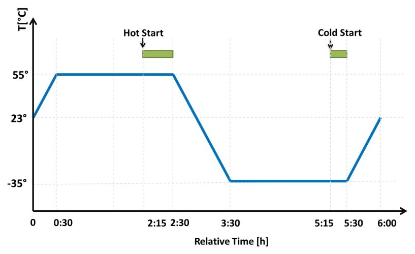
Figure 2 shows coated Flight Model of CHIMERA experiment. The board was successfully tested both functionally and in thermal vacuum chamber. Software running on Flight Model of CHIMERA was tested for more than 150 hours. Figure 3 presents test setup for TVAC test and Figure 4 show temperature profile with Hot/Cold case included.
The CHIMERA board was also a testbed for YGT activity called “Avionics reference designs based on microcontrollers – latch-up protection of COTS memories” that covered the design , characterization, validation of the latch-up protection circuit. Figure 5 shows typical latch-up event and the protection circuit behaviour.
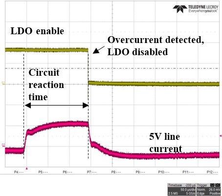
Our circuit successfully protected the memory every time, and the time it took between the occurrence of the latch-up event and the moment when the power to the memory was shut down (called the circuit reaction time) is illustrated in Figure 5