The GaN cookbook
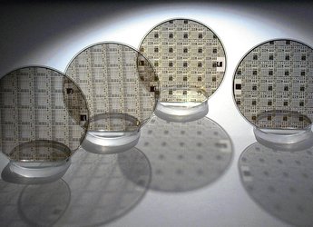
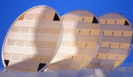
The GaN material used to create working transistors is fabricated layer-by-microscopic-layer using precise mixtures of different gases flowing into a reaction chamber.
“You start off with the ‘substrate’ foundation,” says Mr Barnes. “Ideally, the best match is obviously growing GaN transistors on a GaN substrate, because they have an identical crystal lattice structure. Lattice mismatches and other defects affect the crystal quality, which is strongly linked to device performance and reliability. However, large GaN wafers are still too costly. Instead, we have to use non-lattice-matched material; silicon carbide is the current favourite, closely followed by silicon because of its low cost.
“You also want to grow on a material that has a very high thermal conductivity to dissipate any heat generated and that can be produced in large diameters for low-cost manufacturing.
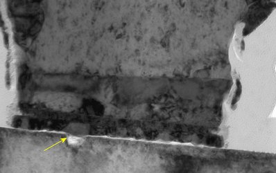
“You use gases to grow a fairly thin high-purity mono-crystalline layer of GaN, ranging from typically one to two microns (a millionth of a metre) thick. Next, you change the chemistry to make a separate layer of aluminium gallium nitride (typically 15–25 nanometres – a billionth of a metre – thick). These two layers, with ‘dielectric passivation’ adding an insulation layer to the device surface, form the basic transistor layer structure. Metallisation depositions are needed to make electrical contacts, and to form the transistor gate and further interconnects.
“Finally, the wafer is turned over and reduced in thickness in order to establish electrical source and ground links through holes that connect the front face to the back. That means grinding the wafer down from typically 400 microns to 100 microns and chemically etching around 50 micron-diameter holes, a non-trivial problem because silicon carbide is a very hard material.’
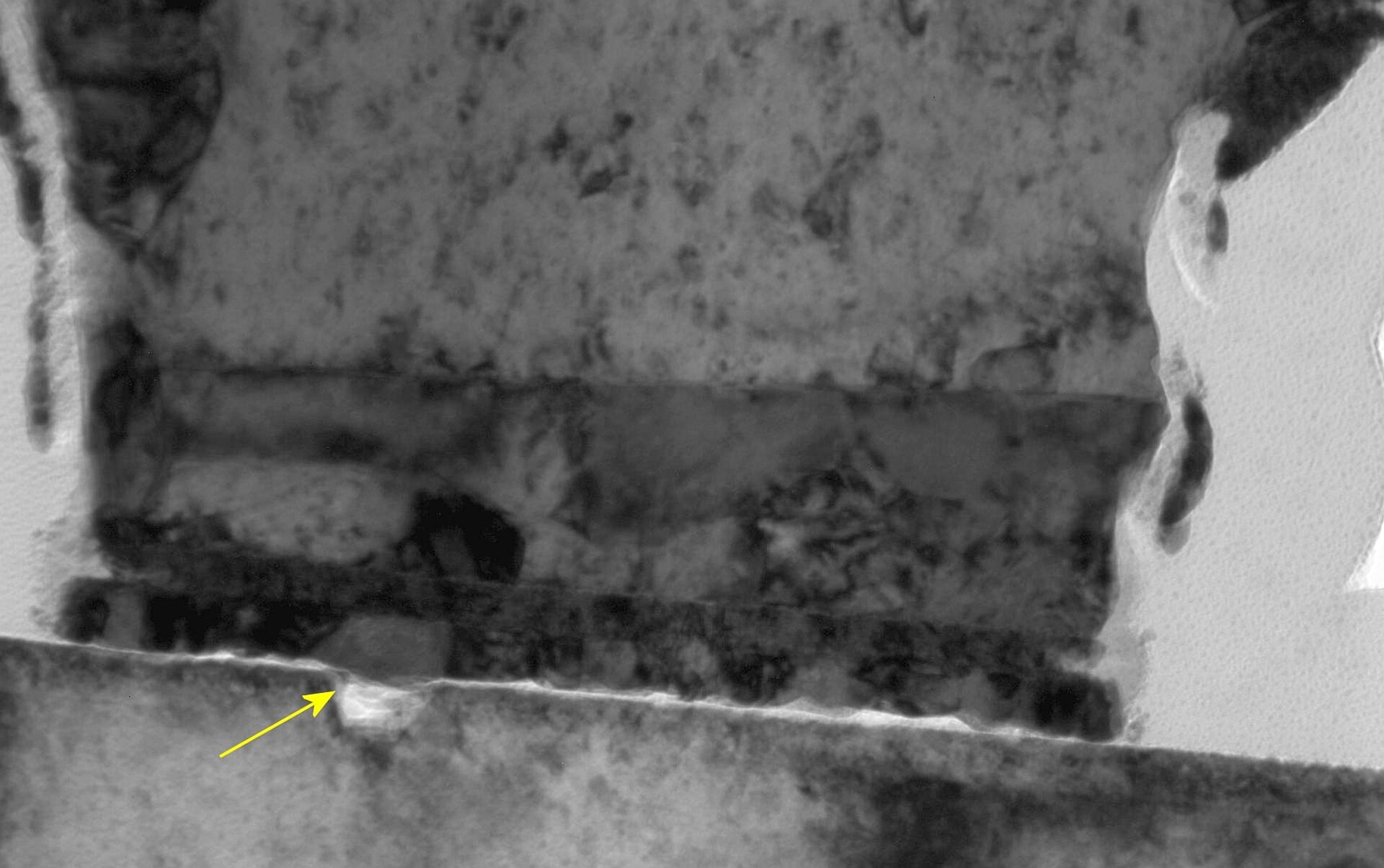
“Today, it can take typically three to four months to fabricate a batch of GaN devices, and the threat of lattice mismatch, crystal strain or other defects is high. Everybody has their own cookbook recipes for minimising this,” says Mr Barnes. “But if defects and surface passivation layers are not properly controlled, you are likely to get rapid degradation in device performance.”
Repeatability of one good wafer run to the next and the transfer from a laboratory environment to product industrialisation are crucial. So GREAT2 is tackling these issues to ensure reliable GaN technology and to optimise the GaN production process.
The intrinsic radiation hardness needs to be maintained whatever the final recipe. GaN products also need to be proofed against prolonged exposure to high vacuum, where outgassing or related ‘hydrogen poisoning’ effects may affect reliability in space.
More information
Andrew.Barnes @ esa int